|
|
Fundamentals of
Layout Design for Electronic Circuits
ISBN
978-3-030-39283-3,
eBook ISBN 978-3-030-39284-0 |
|
|
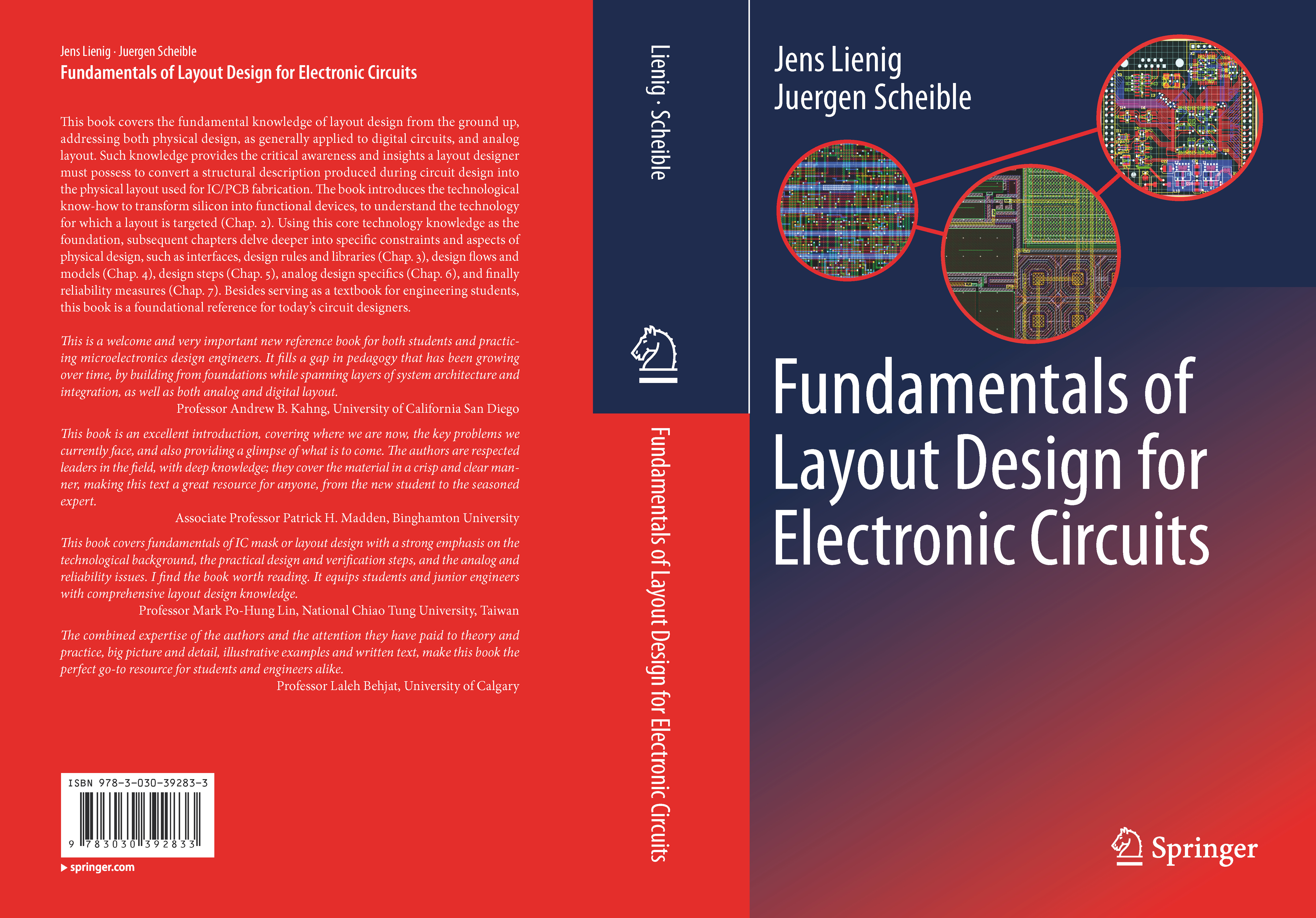
This book covers the fundamental knowledge of layout design from the ground up, addressing both physical design, as generally applied to digital circuits, and analog layout. Such knowledge provides the critical awareness and insights a layout designer must possess to convert a structural description produced during circuit design into the physical layout used for IC/PCB fabrication. The book introduces the technological know-how to transform silicon into functional devices, to understand the technology for which a layout is targeted (Chap. 2). Using this core technology knowledge as the foundation, subsequent chapters delve deeper into specific constraints and aspects of physical design, such as interfaces, design rules and libraries (Chap. 3), design flows and models (Chap. 4), design steps (Chap. 5), analog design specifics (Chap. 6), and finally reliability measures (Chap. 7). Besides serving as a textbook for engineering students, this book is a foundational reference for today’s circuit designers.
Cover Foreword/Preface Table of Contents Index Flyer Errata
Chapter Slides
Chap. 1 Chap. 2 Chap. 3 Chap. 4 Chap. 5 Chap. 6 Chap. 7
Note to lecturers: Chapters 1-7 are well structured for teaching a two-semester class of layout/physical design. For use in a one-semester class, Chap. 1 (introduction) and Chap. 2 (technology) can be assigned for self-study, with instruction starting with Chap. 3 (interfaces), followed by design methodologies (Chap. 4) and design steps (Chap. 5). Alternatively, Chap. 4 can also be used as an effective starting point, followed by the detailed design steps of Chap. 5, intermittently extended with material from the respective interfaces, design rules and libraries presented in Chap. 3.
Contents
1 Introduction This chapter gives a sound introduction to the technologies, tasks and methodologies used to design the layout of an electronic circuit. In Sect. 1.1, we introduce several of the most common fabrication technologies for electronic systems. The central topic of this book is the physical design of integrated circuits (aka chips, ICs) but hybrid technologies and printed circuit boards (PCBs) are also considered. In Sect. 1.2 of our introduction, we examine in more detail the significance and peculiarities of this related branch of modern electronics – also known as microelectronics. In Sect. 1.3, we then consider the physical design of both ICs and PCBs with a specific emphasis on their primary design steps. After these opening sections, we close the introductory chapter in Sect. 1.4 by presenting our motivation for this book and describing the organization of the chapters that follow. 1.1 Electronics Technologies 1.2 Integrated Circuits 1.3 Physical Design 1.4 Motivation and Structure of This Book
2 Technology Know-How: From Silicon to Devices We discuss the fabrication technologies for IC chips in this chapter. We will focus on the main process steps and especially on those aspects that are of particular importance for understanding how they affect, and in some cases drive, the layout of ICs. All our analyses in this chapter will be for silicon as the base material; the principles and understanding gained can be applied to other substrates as well. -- Following a brief introduction to the fundamentals of IC fabrication (Sect. 2.1) and the base material used in it, namely silicon (Sect. 2.2), we discuss the photolithography process deployed for all structuring work in Sect. 2.3. We will then present in Sect. 2.4 some theoretical opening remarks on typical phenomena encountered in IC fabrication. Knowledge of these phenomena is very useful for understanding the process steps we cover in Sects. 2.5-2.8. We examine a simple exemplar process in Sect. 2.9 and observe how a field-effect transistor (FET) – the most important device in modern integrated circuits – is created. To drive the key points home, we provide a review of each topic at the end of every section from the point of view of layout design by discussing relevant physical design aspects. 2.1 Fundamentals of IC Fabrication 2.2 Base Material Silicon 2.3 Photolithography 2.4 Imaging Errors 2.5 Applying and Structuring Oxide Layers 2.6 Doping 2.7 Growing and Structuring Silicon Layers 2.8 Metallization 2.9 CMOS Standard Process
3 Bridges to Technology: Interfaces, Design Rules, and Libraries Having presented fabrication technology for IC chips in Chap. 2, we now investigate in detail an important aspect of the physical design process: data interfaces. We introduce circuit, layout and mask data structures, that is, the main input and output data in the design steps, in this chapter. First, we explain the input to physical design – circuit data – while focusing on schematics and netlists (Sect. 3.1); we then discuss the output of the physical design step: layout data such as layers and polygons (Sect. 3.2). Mask data, which are the data required by the foundry and generated at the end of the design process, are described in Sect. 3.3. Here, we introduce “layout post processing”, where amendments and additions to the chip layout data are performed in order to convert a physical layout into data for mask production. -- Technology data, provided by the chip manufacturing foundry, are crucial for producing the physical design. An important portion of these data are technological constraints which are modeled in the geometrical design rules used in physical design. Essentially, geometrical design rules are constraints for physical design, whose compliance ensures the manufacturability of the layout results. Geometrical design rules are presented in detail in Sect. 3.4. -- Technology data are organized in libraries. These libraries, which are extensively used in IC and PCB design, are covered in our final Sect. 3.5. 3.1 Circuit Data: Schematic and Netlists 3.2 Layout Data: Layers and Polygons 3.3 Mask Data: Layout Post Processing 3.4 Geometrical Design Rules 3.5 Libraries
4 Methodologies for Physical Design: Models, Styles, Tasks, and Flows In Chap. 2 we covered technologies and in Chap. 3 we saw how these technologies interface with physical design. Here in Chap. 4 we now provide an end-to-end overview of the physical design process, namely how to physically construct the layout of an electronic circuit. In this chapter we present the fundamental knowledge an engineer must possess to carry out this task. In Chap. 5 we then discuss each of the specific physical design steps in further detail. -- We begin the chapter by introducing the design flow (Sect. 4.1), design models (Sect. 4.2) and design styles (Sect. 4.3). Next, we investigate various design tasks and related tools (Sect. 4.4), before discussing optimization goals and design constraints (Sect. 4.5). Up to this point our treatise has focused mainly on the digital design flow. In Sect. 4.6 we introduce the characteristics of, and differences between, analog, digital, and mixed-signal design flows. Looking toward the future, we conclude the chapter by presenting two different yet complementary visions for analog-design automation to overcome the analog-digital design gap (Sect. 4.7). 4.1 Design Flows 4.2 Design Models 4.3 Design Styles 4.4 Design Tasks and Tools 4.5 Physical Design Optimization and Constraints 4.6 Analog and Digital Design Flows 4.7 Visions for Analog Design
5 Steps in Physical Design: From Netlist Generation to Layout Post Processing Due to its complexity, the physical design process is divided into several primary steps. Having introduced in Chap. 4 the flow, constraints and methodologies of today’s physical design process, we now investigate the various steps required to generate its output: a layout. These steps, which transform a netlist into optimized mask data, are dealt with one by one in this chapter. -- A layout is generated from a netlist. We first describe how a netlist is created, that is, either by using hardware description languages (HDLs) in digital design (Sect. 5.1), or by deriving it from a schematic, as is common in analog design (Sect. 5.2). Then the physical design steps, comprising partitioning, floorplanning, placement, and routing, are presented in detail (Sect. 5.3). All of these steps are supported by highly sophisticated EDA tools in the case of digital designs, which is our focus here. We also discuss in this section the key aspects of symbolic compaction, standard-cell design and PCB design. -- When the physical design phase is completed, the resulting layout must be verified. This verification step confirms both functional correctness and design manufacturability. Methodologies and tools for comprehensive design verification, with a focus on physical verification, are covered in Sect. 5.4. Finally, we briefly touch on layout post-processing methodologies, such as resolution enhancement techniques (RET), that might impact physical design (Sect. 5.5). 5.1 Generating a Netlist Using Hardware Description Language 5.2 Generating a Netlist Using Symbolic Design Entry 5.3 Primary Steps in Physical Design 5.4 Verification 5.5 Layout Post Processing
6 Special Layout Techniques for Analog Design While the physical design steps introduced in Chaps. 4 and 5 are universal, analog integrated circuits present further challenges that require additional layout techniques. There are many differences between analog and digital, and as such, the design flows and tools vary in both cases. Analog circuits are generally less complex in terms of transistor count and are designed in a manual fashion. The distinct lack of design automation means that manual design is still in widespread use today, requiring specialist knowledge that is unique to analog design. This specialist knowledge is covered in this chapter. -- We discussed analog design flows in Chap. 4 (Sects. 4.6, 4.7), previously. Now we present layout techniques that accompany these analog flows, which an analog layout designer must be fully aware of. We start with an introduction to sheet resistances and wells (Sects. 6.1, 6.2) as this knowledge is needed for the sizing and understanding of analog devices, which we then cover in Sect. 6.3. The methodology for cell generators, which produce such analog devices, is presented in Sect. 6.4. An explanation of the fundamental importance of symmetry and a treatise of resulting matching concepts (Sects. 6.5, 6.6) conclude this chapter. 6.1 Sheet Resistance: Calculating with Squares 6.2 Wells 6.3 Devices: Layout, Connection, and Sizing 6.4 Cell Generators: From Parameters to Layout 6.5 The Importance of Symmetry 6.6 Layout Matching Concepts
7 Addressing Reliability in Physical Design Reliability of electronic circuits is becoming an increasing concern due to the ongoing downscaling of the structural dimensions and the continuous increase in performance requirements. This final chapter addresses the many options available to a layout designer, given the enormous influence of physical design on circuit reliability. Hence, the goal of this chapter is to summarize the state of the art in reliability-driven physical design and related mitigating measures. -- We start by presenting reliability issues that can lead to temporary circuit malfunctions. We discuss in this context parasitic effects in the bulk of silicon (Sect. 7.1), at its surface (Sect. 7.2), and in the interconnect layers (Sect. 7.3). Our main goal is to show how these effects can be suppressed through appropriate layout measures. -- After having presented temporarily-induced malfunctions and their mitigation options, we discuss the growing challenges of preventing ICs from irreversible damage. This requires the investigation of overvoltage events (Sect. 7.4) and migration processes, such as electromigration, thermal and stress migration (Sect. 7.5). Again, not only do we discuss the physical background to this damage, we also present appropriate mitigation measures. 7.1 Parasitic Effects in Silicon 7.2 Surface Effects 7.3 Interconnect Parasitics 7.4 Overvoltage Protection 7.5 Migration Effects in Metal
|
||
| Impressum | ||
| Last update: 09.05.2024 | ||